by
Applications Engineering Staff
0-02 Fair Lawn Avenue - Fair Lawn, NJ 07410
This paper describes a high-current, high-power family of hermetic packages with regard to thermal performance and reliability. The configurations and material components are then explained in relation to the external size and room available for additional components in the internal cavity. Thermal resistance measurements and calculations are given for a large power transistor in addition to a ceramic-mounted diode and power-FET assembly. A brief description is provided of the instrumentation used to make thermal resistance measurements. Future packages under development are also described.
Often new packages are perceived with some disregard by power electronics circuit designers because there is no apparent benefit to circuit functions. This is true. The benefits, though real and tangible, are not always apparent.
Improved packaging almost always results in thermal benefits. In this case the reduction of losses from lower thermal resistance and diminished lead resistance show up as a savings in the power budget and will be interpreted as an efficiency improvement. In mathematical terms, the relationship follows from the equation Tj - Tc + Pd*Rqjc. If the new package provides a lower Rqjc, then Tj will be reduced. On the other hand, the savings could be applied to the heat-sink size such that Tc would increase while Tj remained unchanged. Another option would be to apply the savings to an increase in Pd, allowing the usage of transistors with higher saturation voltages.
Improved packaging also provides electrical benefits. A reduction of lead resistance will give more output signal to the load. This is especially noticeable in circuits operating at 50 Amps and above. Also, a reduction of thermal resistance allows semiconductors to operate at lower temperatures, thus improving circuit operation.
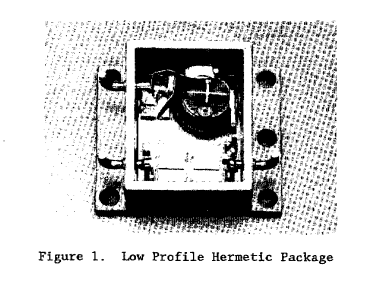
The new LPH package (Low Profile Hermetic, see Figure 1) provides the advantage of low thermal resistance and low lead resistance as discussed above. It also has other advantages for a package of this size [0.6in.(1.5cm.)xl.7in.(4.3cm.)xl.95in.(4.95cm.); 4.Oozs.(115gms.)]. It mounts and connects from one side of the heat-sink. It has 90 mil pins which conduct currents up to 150 Amps. The glass seals provide 1000 Volts (RMS) isolation. The package has a post-weld hermeticity of 5.OxlOexp-7 atm-cc/sec. Unlike some packages presently in the marketplace, the LPH consistently shows excellent yields under the high reliability screen. This consists of the following:
*Although these are primarily electrical tests, they are included here because they stress the package.
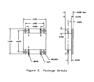
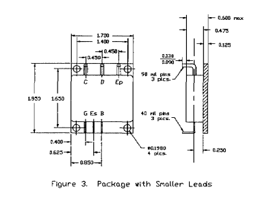
The basic package structure consists of a baseplate, which is brazed to a frame (See Figure 2). The leads are 90-mil diameter copper-cored Kovar. The glass seals are 200 mils in diameter and are compression-sealed into position. The package is designed to accept six of these large leads, leaving adequate room for solder connections. Smaller leads, however, may also be used, allowing an increase of pin count to greater than six (See Figure 3). The 90-mil leads, as designed, have a resistance of 25 microohms, which keeps electrical and thermal insertion losses to a bare minimum.
Welding is achieved with a parallel-seam sealer mounted in a nitrogen-filled glove box. The package lid is designed to prevent "oil-canning" while allowing for a reliable weld. The entire package receives an electroless plate followed by gold over the pins only. The gold enhances the solderability of the pins, for both connection of the internal components and for customer connections at assembly.
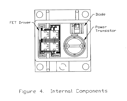
The internal cavity of the LPH package is 1.5in.(3.Bcm.)xl.lin.(2.8cm.) or 1.65 square inches, which allows for several combinations of components to build up sub-circuits. Components used are typically diodes, FET's and power transistors. All components are mounted on alumina or beryllia to provide isolation from the case. Great flexibility of sub-circuit design is achieved for mounting drive and protective circuitry. An example of one typical circuit is shown in Figure 4 in which a FET drive circuit is mounted on a ceramic substrate to one side of the cavity. The remaining space is dedicated to power components. The power diode is also mounted on a ceramic substrate.
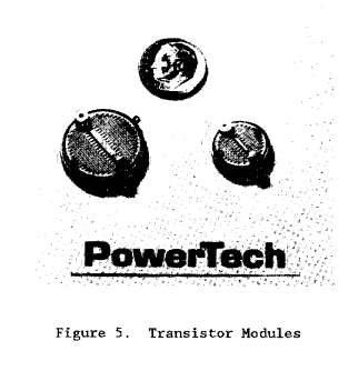
The transistors under discussion have been designed in two sizes: 570 mils in diameter and 816 mils in diameter. The two modules are shown in Figure 5. The ratio of silicon on the 816-mil device to the 570-mil device is two to one. Thus the 816-mil unit has about double the current rating of the smaller device.
The devices are manufactured by either the single-diffused method, resulting in a choice of low-voltage (<200 volts), ultra-high current (up to 500 amps) or by the triple-diffused method resulting in high-voltage (up to 600 volts) and high current (up to 150 amps). The transistor chip (silicon) is mounted to a heat-spreader which is a moly disc brazed to a copper disc. This assembly is referred to as the transistor module. A proprietary attachment technique is used to mount the silicon to the moly, assuring a void-free connection. The moly provides an excellent match of thermal expansion coefficient to the silicon and reduces thermal stress on the solder joint. The copper disc provides effective heat spreading, increasing the thermal. conductivity from the silicon junction to the outside world. In order to adapt the transistor module to the LPH package, a vertical copper tab has been added to the copper disc to serve as the collector terminal. The transistor module assembly and an isolation disc are then stacked and mounted into the LPH package. This provides the isolation necessary to keep the package at ground potential.
Since all the mechanical components in the transistor assembly are circular, the following analysis was used to calculate the thermal resistance from the silicon chip to the outside surface of the LPH package. Calculated and measured values of thermal resistance are shown in Table 1 for each component of the transistor module assembly. Thermal resistance for circular materials is calculated from the equation 9 = 1.27t/kd(d*2t) where t is the thickness in centimeters, d is the diameter in centimeters at the top surface of each component normal to the direction of heat flow, and k is the thermal conductivity in joules*cm/(cm*cm*sec*degC) of each material at IOOC. This equation allows for heat spreading which is assumed to be 45 degrees. Platings, coatings, and metallizations have been omitted from the calculations since their thermal resistances are negligible. Since the components for each transistor-module design are of the same thickness and material, their thermal resistances vary by the ratio of their areas. The resulting calculated junction-to-case thermal resistance then becomes 0.271 C/W for the small chip and 0.135C/W for the large chip. The measured values of 0.295 and 0.161 are in close agreement with the calculations, thereby providing the confidence that is necessary for design acceptance.

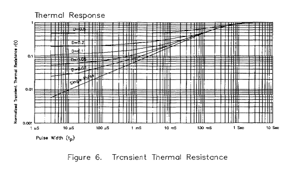
A normalized curve of transient thermal resistance is shown in Figure 6. This can be used for each isolated chip in the LPH-150 package. Data for this curve and steady-state thermal resistances are measured on a thermal resistance tester designed and built specifically for evaluation of these devices.
Two methods of mounting components that are commonly required are:
These chips range in size from 1/16 in. per side to 1/4 in. per side.
Since these chips have a square profile, thermal resistance is calculated from the equation 8 - t/kd(d+2t) where t is the thickness in centimeters, d is the length in centimeters of one side of the component,
and k is the thermal conductivity in joules*cm/(cm*cm*sec*degC) of each material at 100C. This equation allows for heat spreading which is assumed to be 45 deg.
Calculated values of thermal resistance are shown in Table 2 for each component of the power-chip assembly. Two square chips are investigated; 5/32 in., and 1/4 in. for each type of construction as discussed above. As with the transistor's thermal resistance, the measured results shown in Tables 2A and 2B are in close agreement, testifying to the acceptability of the design.

Measurements are made on proprietary equipment designed and built to be compatible with Mil Std 750, Methods 3132 and 3161. Prior to testing, the portion of the semiconductor that is to be used for thermal sensing is measured for its temperature coefficient of voltage at the monitor current.
This is the base-emitter junction for bipolar transistors, the reverse body diode for FET's and the forward junction for diodes. The thermal resistance tester measures these parameters at the same monitor current immediately before and immediately after application of the power pulse. The tester utilizes an IBM AT computer with an analog input board to measure the monitor current, the test current through the device under test (DUT), and the test voltage across the DUT. The temperature coefficient of voltage is entered at the start of testing along with the test current and voltage. At the completion of test, the tester provides temperature rise in degrees C, power dissipation in watts, the actual test voltage and current and a calculated thermal resistance in C/W. The DUT is mounted to a water-cooled heatsink to hold the case at 25C. Typically it holds it at 23C at both the start and end of a one-second test. The computer program also accepts this temperature and uses it to calculate the DUT's junction temperature at the end of test.
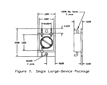
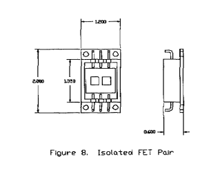
The wish-list of power packages can be endless, but development effort is continuing to provide additional packages of similar design that match current and future market requirements. The first, shown in Figure 7, efficiently and hermetically houses the large 816-mil transistor chip and continues to provide all of the advantages cited for the LPH package. Its major advantage however, is its size since it houses either a 500-amp single-diffused device or a 150-amp triple-diffused transistor. The second package (see Figure 8) has the same form factor as the first, but smaller pins and corner hole mounting permit isolated mounting of a pair of power FETS.
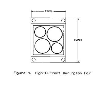
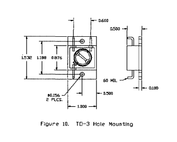
Other device combinations are also possible here. The third package (see Figure 9) is sized for a high-current Darlington pair where one Darlington consists of the small chip driving the large chip. Ratings here are similar and with the same advantages for a hermetic package as described above. The fourth package (See Figure 10) was developed to mount in TO-3 hole spacings with the added advantages of internal isolation, lower thermal resistance and one-side mount/connect accessibility. It is of a slightly larger and different shape than the TO3 package, however.